
Explore ASML and ZEISS Hyper-NA EUV: 13.5 nm light, ultra-precise mirrors, numerical aperture and manufacturing challenges for future AI chips.
Smaller features, a larger industrial challenge
One of the machines that matters most to artificial intelligence does not resemble a computer. It combines invisible light, optics, motion, sensors and thermal control to transfer microscopic patterns to a silicon disc. The chip reaching its user is the outcome of an industrial chain, with lithography as one of its decisive steps.
In an EUV system, a mask pattern is projected onto photosensitive material on a wafer. Light at 13.5 nm travels through mirrors in vacuum. Numerical aperture contributes to resolving detail, but materials, focus, alignment and process control must keep pace with the optics.
Reuters reported a roughly ten-year development horizon for Hyper-NA on 8 October 2026. That is an expectation, not a product launch. This article explains what the proposal changes and what must still be demonstrated to turn optical resolution into reliable manufacturing. Last updated: 8 October 2026.

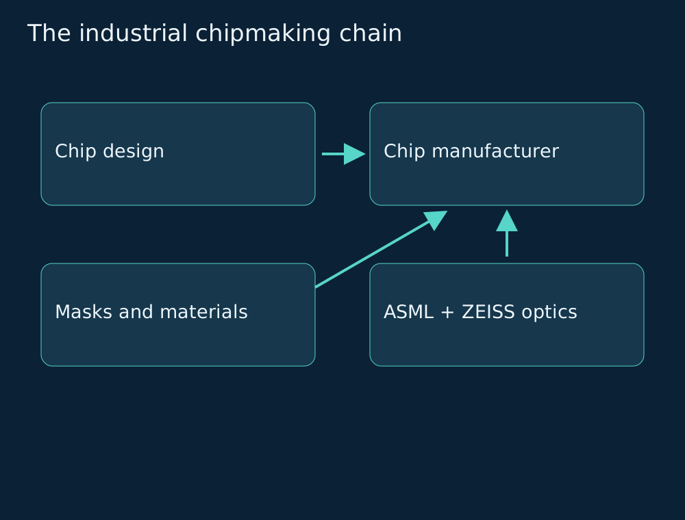
What are ASML and ZEISS, and who actually makes the chip?
ASML integrates and supplies lithography systems, including equipment, software and services. ZEISS develops and manufactures critical optics within the imaging chain. Supplying an exposure tool and operating a chip factory are different activities: semiconductor manufacturers must integrate many tools and qualify a complete process.
Intel, Samsung and TSMC participate as chip manufacturers, with different business models and processes. Imec works in applied research and process development. The joint ASML-imec High-NA laboratory illustrates why scanners, materials and metrology must develop together.
These roles help interpret a technology announcement. A viable mirror is not a validated scanner; a delivered scanner does not mean every layer of a product has been qualified. Integration, yield, availability and economics stand between a demonstration and production. These are complementary engineering milestones rather than administrative details.
ASML · How microchips are made →
ASML / imec · ASML and imec open joint High NA EUV Lithography Lab — 3 June 2024 →
How is a microchip manufactured?
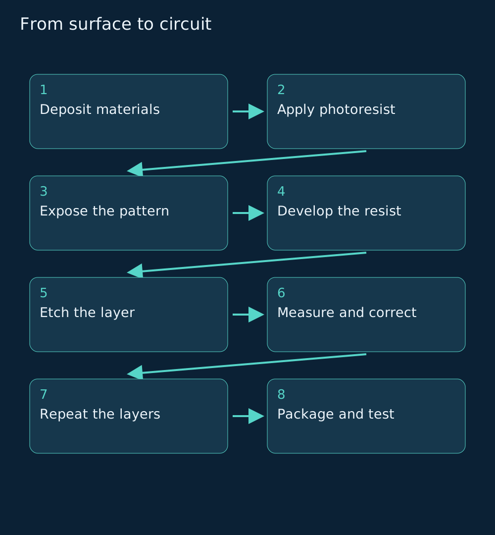
A wafer is a semiconductor disc that provides the base for many circuits. Processes deposit thin films and modify materials on it. Photoresist, or resist, is sensitive to exposure; the reticle, also called a photomask, carries the pattern that the imaging system transfers.
An educational sequence is to deposit a layer, coat resist, expose a pattern, develop the resist, transfer it by etching, inspect and repeat. Actual sequences depend on the layer and may include other operations. Development creates the resist pattern; etching transfers that pattern into the underlying material. Confusing those functions hides an important part of manufacturing.
Testing and packaging eventually integrate the circuits into a product. Lithography does not deliver a finished processor in a single exposure. Think of building in layers: each step must preserve previous work and leave an appropriate condition for the next. The industrial challenge is repeating that sequence while keeping defects and variation under control.
How do a laser and tin droplets produce EUV light?
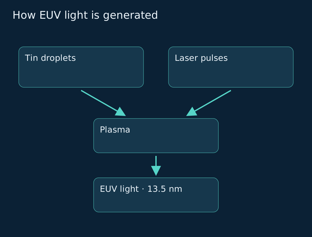
EUV means extreme ultraviolet. The systems discussed here use a wavelength of 13.5 nanometres, with a nanometre equal to one billionth of a metre. Advanced DUV systems also use 193 nm light. Wavelength contributes to imaging scale but is not the literal size of every printed element.
In the source described by ASML, laser pulses strike tin droplets: one prepares the droplet and another creates plasma that emits EUV radiation. Collected light feeds the illumination and imaging chain. The laser does not directly draw a transistor on silicon. Generating radiation and forming the pattern are distinct functions.
This distinction explains the performance challenge. Generating light energy is insufficient unless the exposure process can use it appropriately. Source stability, optical losses and operating conditions all contribute. Improving one module has industrial value only when the rest of the chain can take advantage of that improvement.
Why does EUV use mirrors instead of lenses?
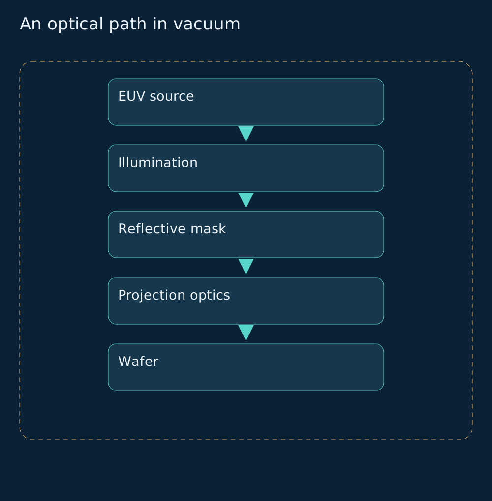
Air and common materials strongly absorb EUV light. Its path therefore operates in vacuum and uses multilayer mirrors, including a reflective mask. Illumination, mask and projection optics form the pattern together, rather than light passing through an ordinary lens as in a domestic projector.
Mirror coatings are engineered for the spectral band and angular conditions of the application. Surface shape, coating, cleanliness and positioning must work together. A smooth surface alone does not ensure the required image. ZEISS has a central role because manufacturing and verifying these optics requires its own substantial engineering chain.
ZEISS describes High-NA projection optics with more than 40,000 parts and a mass of approximately twelve tonnes. Those figures concern existing High-NA technology, not Hyper-NA specifications or the total mass of a scanner. They show the scale of integration: large structures must preserve extremely stable geometric relationships.
What does numerical aperture mean in lithography?
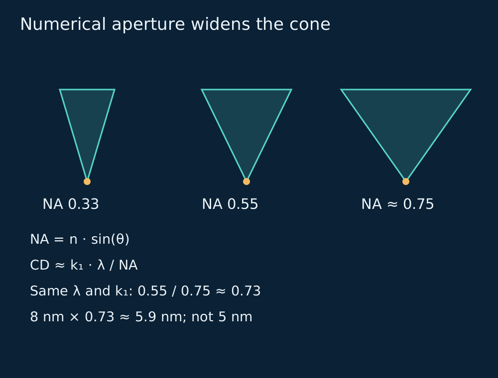
Numerical aperture, or NA, describes the angular range accepted by the optics; in vacuum it relates to the sine of the cone’s half-angle. A wider range captures spatial information that helps resolve finer detail. A camera analogy is helpful provided the concept is not reduced to simply collecting more light intensity.
The educational Rayleigh model is CD ≈ k₁ × λ / NA. CD means critical dimension, λ is wavelength and k₁ summarises imaging and process factors. Holding λ and k₁ constant, changing NA from 0.55 to 0.75 gives a ratio of 0.55/0.75 ≈ 0.73: the theoretical dimension would be about 27% smaller. This is an idealised calculation, not a product measurement.
Applied directly to an 8 nm reference, that ratio gives approximately 5.9 nm rather than 5 nm. Discussion of features close to 5 nm involves particular imaging and process conditions. The equation explains a trend; it cannot replace measurements or establish that every circuit structure will share one dimension.
How do EUV, High-NA and Hyper-NA differ?
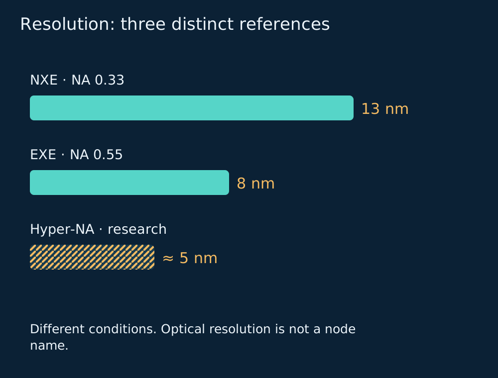
ASML distinguishes NXE systems with NA 0.33 and 13 nm resolution from EXE systems with NA 0.55 and 8 nm resolution. Both use 13.5 nm EUV light. Hyper-NA investigates increasing aperture to approximately 0.75 or above while retaining that wavelength. High-NA and Hyper-NA therefore are not alternative spellings of one machine.
The table summarises resolution references and development status. It does not compare commercial process nodes or specify an entire fabrication process. Generations may coexist within a factory and across different layers of a product. Tool selection depends on the pattern, manufacturing strategy and economic outcome of integration.
A sound comparison also distinguishes resolution, exposure field, throughput and yield. Knowing that a tool can form a smaller feature does not tell us how many functioning chips it will deliver in a shift. Industrial decisions must combine optical capability with process window and factory operation.
ASML · EUV lithography systems — NXE and EXE →
| Characteristic | EUV / NXE | High-NA / EXE | Hyper-NA / proposal |
|---|---|---|---|
| Numerical aperture | 0.33 | 0.55 | ≈0.75 or above |
| Wavelength | 13.5 nm | 13.5 nm | 13.5 nm in the studied path |
| Resolution reference | 13 nm (ASML) | 8 nm (ASML) | ≈5 nm, potential under specific conditions |
| Status | Established production | Existing equipment; industrial qualification and adoption | Research; no confirmed commercial launch |
| Additional demands | EUV integration | Optics, field and focus | Focus, masks, resist and yield |
Do 5 nm features mean a 5 nm process node?
No. Resolution or feature size describes patterning capability under defined conditions. A process-node name refers to an industrial generation rather than one physical dimension shared by all transistors. A chip combines structures of different shapes and sizes with architectural and integration choices.
That explains why ASML’s tables connect optical resolution to products with differently named nodes. Research targeting approximately 5 nm features does not mean returning to the commercial 5 nm node, nor demonstrating a complete transistor with every dimension equal to that number.
When reading a claim, look for the measurement definition. Is it line width, half-pitch, spacing, critical dimension after etching or a process name? Which pattern and material were used? Without those conditions, two values with the same units may describe quite different results.
What does the Hyper-NA proposal add?
The April 2026 SPIE proceedings study by Benschop and colleagues evaluates NA around 0.75 at 13.5 nm while retaining the EUV ecosystem. Its abstract discusses mask adjustments, focus control, thin resist and platform integration. The aim is to extend single-exposure capabilities for selected patterns, rather than automatically remove every additional fabrication step.
The October reference is Patra, Feldmann, Neumann and Bottiglieri, “Hyper-NA: a system with a numerical aperture of at least 0.75”, Journal of Micro/Nanopatterning, Materials, and Metrology 25(4), 041807, DOI 10.1117/1.JMM.25.4.041807. We identified its bibliographic reference but could not access the complete text during this check. We do not attribute a set of commercial product specifications to it.
Reusing parts of a platform may reduce industrial disruption. Nevertheless, increasing aperture changes requirements across modules. Evaluation must identify which components remain, which interfaces change and which outcomes have been demonstrated under representative conditions. Technological continuity does not mean straightforward integration.
Why not shorten the wavelength further?
The 13.5 nm path preserves an established infrastructure of sources, materials and optics. The April abstract discusses multilayer-mirror angular bandwidth limitations for a transition to 6.7 nm. The difficulty involves the optical system as a whole: choosing a smaller wavelength does not solve manufacturing by itself.
This does not prove that a shorter-wavelength path will remain impossible forever. It means source, reflection, masks, resist, detection and integration must be reassessed. An alternative can be promising in a laboratory without offering the best industrial transition for a particular generation.
The reasoning is familiar in engineering. Retaining a validated platform is valuable but has limits. Decisions compare benefits and difficulties across complete paths instead of optimising one isolated variable. Better theoretical resolution must meet a workable solution in materials, control and production.
The mechanical heart: speed with stability
During exposure, wafer and reticle stages perform coordinated motion. Useful position is relative: the pattern must land correctly against the surface and previous layers. A stage that is precise in an unsuitable reference frame does not ensure correct product alignment.
Mechatronics combines structures, actuators, sensors and control software. Motion can introduce vibration and heat; thermal changes can alter geometry. The solution requires dynamic control rather than simply manufacturing tight-tolerance parts. Speed and acceleration figures for existing platforms should not be copied as future Hyper-NA specifications.
Consider a maintenance analogy: replacing a component with a nominally compatible one does not establish that the full assembly retains its performance. Stiffness, mounting, calibration and thermal response may matter. In lithography, verification must examine the imaging and positioning chain as well as the replaced module.
Metrology: making it correctly and proving it
Metrology is measurement science applied here to process control. Overlay describes alignment between layers. Focus, critical dimension and defects require appropriate monitoring methods; a visually convincing image is insufficient evidence that a circuit meets its requirements.
ASML describes diffraction-based optical metrology and electron-beam inspection as complementary methods. Measurement supplies correction data; inspection helps locate defects. Optical verification likewise requires calibration and stability. More displayed decimal places do not remove systematic uncertainty.
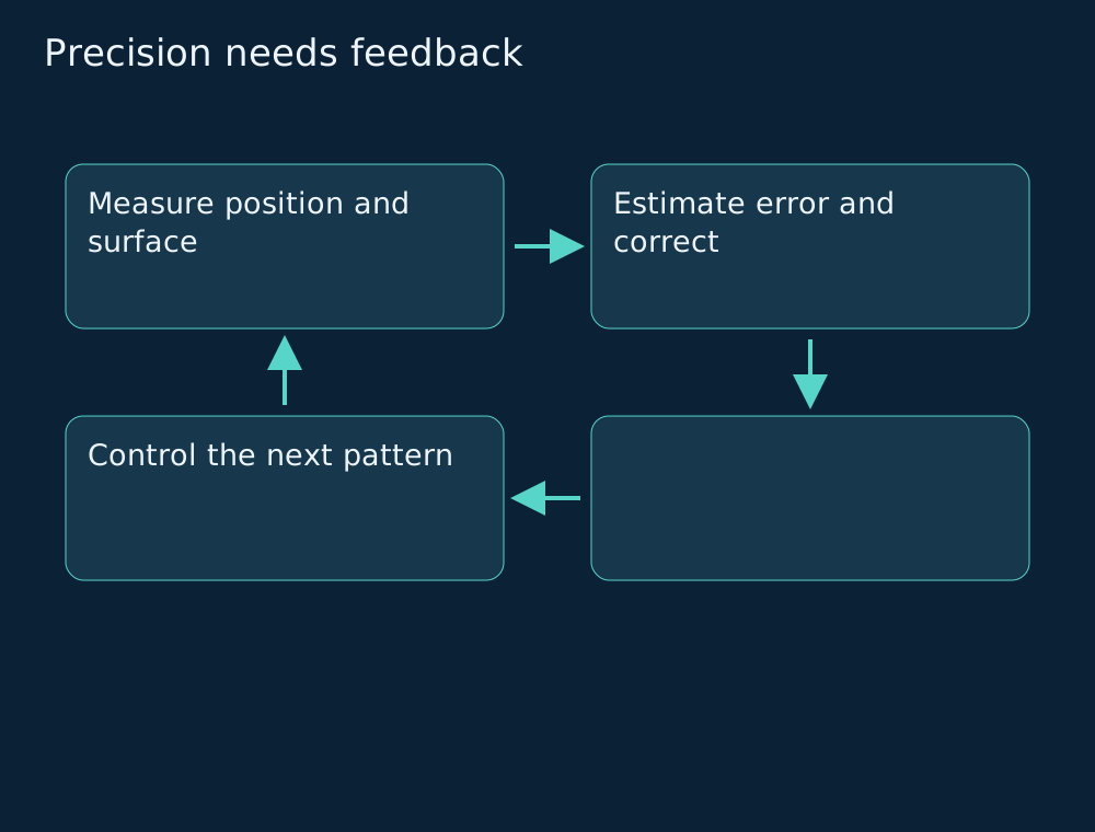
The control loop must close: measure, interpret, correct and verify the effect. An error in a reference system can produce consistent corrections in the wrong direction. Reliability therefore involves sensors, models, configuration and acceptance criteria. What matters is precision demonstrated through repeated process performance.
Focus and photoresist may become the new bottleneck
Increasing NA improves resolution but tends to reduce depth of focus under comparable conditions. The April SPIE abstract discusses focus-control improvement from approximately 35 nm to 20 nm. These are the authors’ assessment, rather than final product specifications or transistor dimensions.
Photoresist also faces trade-offs among resolution, sensitivity and line-edge roughness, or LER. The Chemical Science review by Chu and colleagues describes stochastic effects involving photons, secondary electrons and resist-component distributions. The exposure dose must support both pattern fidelity and useful throughput, with patterns that can survive transfer.
The practical consequence is a narrow process window: several sources of variation must remain acceptable simultaneously. Improving one variable may move the problem elsewhere. Optics, chemistry and height control need joint evaluation. One successful pattern does not establish yield throughout a factory campaign.
Eight challenges between a proposal and a fab
Better optics create opportunities without completing the work. Industrialisation requires evidence for each interface and acceptance conditions for the full arrangement. The eight groups below organise that assessment; they are not a statement that every challenge has already been solved for Hyper-NA.
Success also needs a measurement definition. Throughput describes processing productivity; availability describes usable operating time; yield concerns functioning devices. These metrics interact but are different. A faster tool may fail to lower cost if it increases rework or loses stability during operation.
- Optics: aperture and image quality with usable transmission.
- Masks: three-dimensional effects, angles and absorber materials.
- Focus: surface height and exposure window.
- Resist: thickness, sensitivity, LER and pattern transfer.
- Precision: repeatable motion and overlay across layers.
- Inspection: detecting and characterising relevant defects.
- Economics: throughput, availability, yield and cost.
- Ecosystem: suppliers, materials, software and qualification.
Safety and reliability in precision manufacturing
Manufacturing brings together laser sources, electrical systems, vacuum, moving mechanisms and process chemicals. Hazards depend on equipment and task, particularly during maintenance and configuration changes. Cleanrooms control product contamination; they do not remove the need to protect people.
Interlocks, energy isolation, procedures and qualifications must match actual intervention modes. This is an analysis of engineering principles, not a scanner operating manual or a claim about internal Hyper-NA protections. An editorial image cannot justify inventing a safety circuit.
Precision and safety share a discipline: changes must be controlled and their effects verified. A change affecting alignment or cleanliness can also affect access, movement and maintenance exposure. Risk management follows the system’s configuration and the work actually performed.
When could Hyper-NA enter production?
This edition did not identify an announced commercial Hyper-NA product with a guaranteed delivery date. The roughly decade-long outlook is a development horizon subject to technical outcomes and decisions. It is not a commitment to a specific year or a confirmed adoption schedule for Intel, TSMC or Samsung.
High-NA is an existing generation with equipment and qualification programmes. Hyper-NA is the research step discussed here. Extrapolating from one does not establish the other’s price, sales volumes or throughput. Each assertion needs its own evidence, identifying technology, units, date and context.
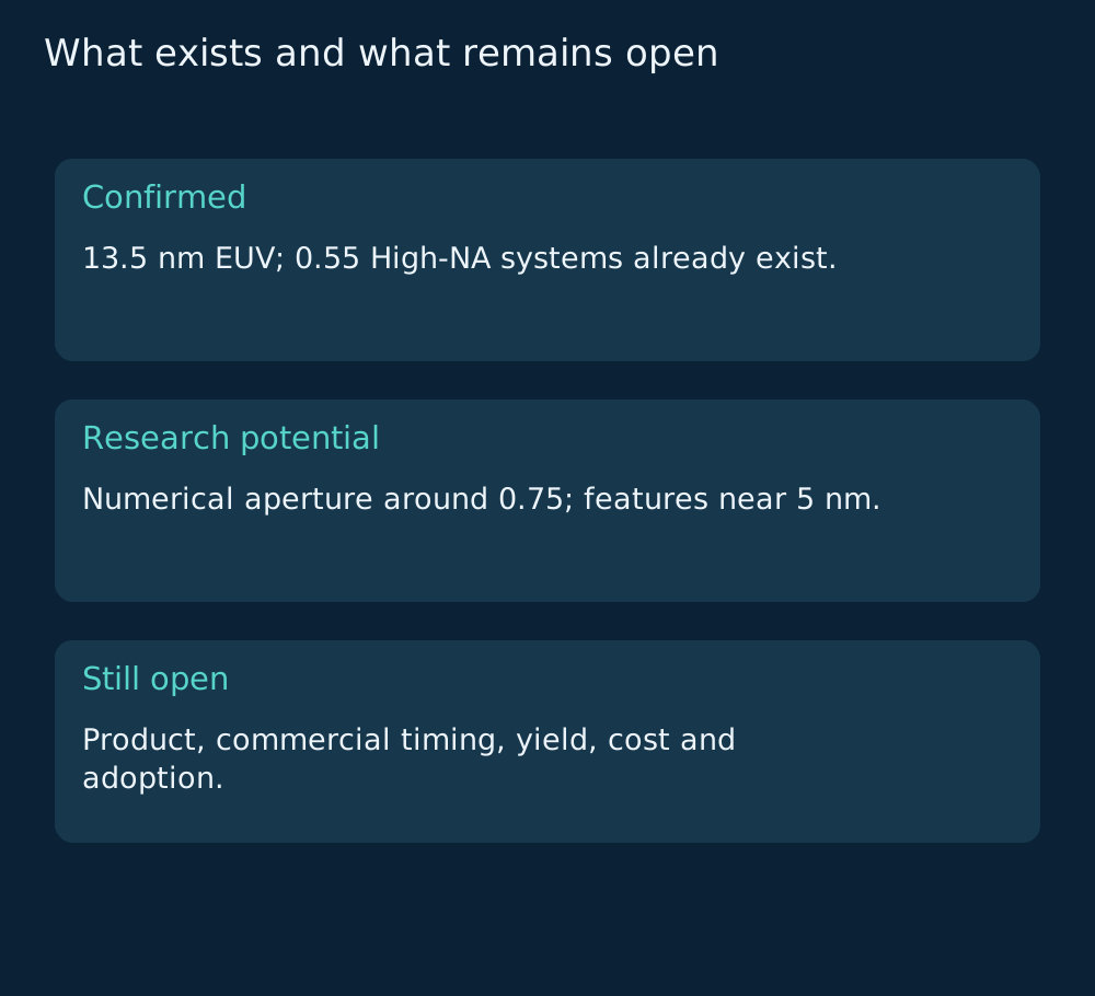
The visual separates confirmed capability, potential and open questions. It supports following developments without treating technological interest as commercial certainty. New findings should update the same analysis: what was demonstrated, under which conditions and with which production-relevant limits still unresolved?
Will Hyper-NA make AI chips more efficient?
Smaller features may broaden density and integration options but do not guarantee a percentage gain in speed or energy use. Performance depends on architecture, memory, interconnects, packaging, software and workload. Lithography helps enable structures; it does not determine AI-model efficiency by itself.
Energy used to manufacture a chip must also be distinguished from energy used to operate it. Fewer steps in a layer may change manufacturing resources, while architecture may change energy per task. A comparison must define useful output and system boundaries. A scanner should not receive credit for a benefit produced by the complete computing design.
This connection gives substance to the idea that AI is physical. Alongside data-centre electricity and cooling are the materials, machines and factories that make processors possible. The related articles below explore those other links while keeping this article focused on lithography and precision engineering.
ASML · How microchips are made →
Brazilian AI data centres: physical infrastructure →
Making the smallest feature requires mastering the whole
Hyper-NA proposes extending optical lithography through a wider aperture. Its importance lies in potential and requirements together: focus, mask, materials, measurement, motion and integration must progress jointly. Every demonstration reduces part of the uncertainty; production requires repeatability across the full system.
Behind AI chips are optics, mechanical engineering, automation, chemistry and specialised professionals. Technology delivers value when it turns physical limits into a reliable process. The smaller the feature we seek to manufacture, the greater the responsibility to verify the combination that makes it possible.
Frequently asked questions
Why is ASML important to chipmaking?
It supplies tools that transfer critical patterns; complete manufacturing depends on many other steps and companies.
What is ZEISS’s role in EUV mirrors?
Developing, manufacturing and verifying the optics that guide radiation and form precise images.
How does an EUV machine work?
A source generates radiation, a mask defines the pattern and optics project it onto wafer resist within a controlled system.
Are EUV, High-NA and Hyper-NA the same?
EUV describes the light technology; High-NA is an existing higher-aperture generation; Hyper-NA investigates a further increase.
Is numerical aperture just light intensity?
No. The accepted angular range matters for spatial information and image resolution.
Does the laser directly print a transistor?
No: it generates tin plasma; the pattern comes from the mask and projection chain.
What does printing roughly 5 nm mean?
A potential feature reference under specific conditions, not an entire transistor or a process-node name.
Is there a guaranteed Hyper-NA launch date?
None was identified in this edition. A research horizon is not a commercial delivery commitment.
Will AI chips automatically become more efficient?
No percentage is guaranteed: gains also depend on architecture, materials, memory, software and manufacturing.
How does resolution differ from a 5 nm node?
Resolution describes patterning under defined conditions; a node identifies a process generation rather than a universal physical dimension.
References
- Patra, Feldmann, Neumann & Bottiglieri — Hyper-NA: a system with a numerical aperture of at least 0.75 · JMM 25(4), 041807 (2026)SPIE / Journal of Micro/Nanopatterning, Materials, and Metrology
- Benschop et al. — Hyper-NA at 13.5nm: a natural next step to extend single-exposure EUV lithography · Proc. SPIE 13979, 139790T (22 April 2026)SPIE
- EUV lithography systems — NXE and EXEASML
- The Rayleigh criterionASML
- Light & lasersASML
- Lenses & mirrorsASML
- High-NA-EUV LithographyZEISS SMT
- Mechanics & mechatronicsASML
- Measuring accuracyASML
- How microchips are madeASML
- Six crucial steps in semiconductor manufacturingASML
- ASML and imec open joint High NA EUV Lithography Lab — 3 June 2024ASML / imec
- Chu et al. — Recent efforts of vapour-phase strategies for EUV resist toward high- and hyper-NA extreme ultraviolet lithography · Chemical Science 17, 11754–11773 (2026)Royal Society of Chemistry
- ASML, Zeiss say next-generation chipmaking technology may be ready in 10 years — 8 October 2026Reuters